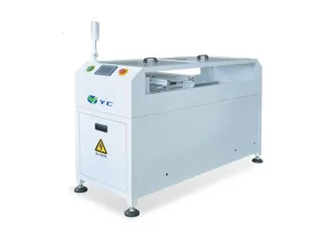
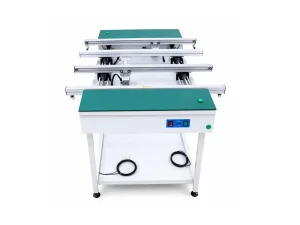
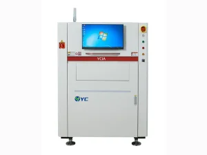
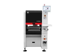
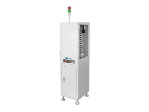
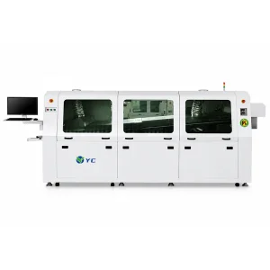
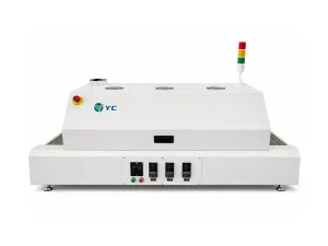
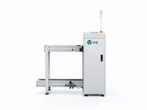
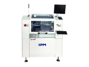
In the era of miniaturization, 3D Solder Paste Inspection (SPI) is no longer an optional luxury but a cornerstone of E-E-A-T compliant manufacturing. As solder joints shrink, the margin for error effectively vanishes. Yichun Electronic provides high-precision SPI solutions that go beyond mere defect detection; they serve as analytical hubs for closed-loop print process optimization.
The industry is shifting from reactive inspection to predictive AI maintenance. Our 3D SPI systems utilize high-speed moiré interferometry to generate volumetric data, which is then fed back to screen printers via M2M (Machine-to-Machine) communication. This digital transformation reduces scrap rates by up to 90% in high-mix environments.
China remains the undisputed epicenter of SMT manufacturing, offering a unique blend of vertical integration and rapid scalability. By sourcing SPI equipment from Yichun, global manufacturers gain access to:
2D systems only measure area. 3D SPI measures volume, height, and coplanarity, which are critical for preventing micro-solder defects on 01005 components.
We provide remote engineering diagnostics, onsite installation, and dedicated training modules to ensure your team achieves full operational autonomy.
Yes, our systems follow standard SMT communication protocols (e.g., IPC-CFX, SMEMA), ensuring seamless integration into existing lines.
 Yichun Electronic