Explore our industrial-grade SMT assembly machinery, including high-speed pick and place systems, 3D SPI inspectors, reflow ovens, and intelligent conveyor systems engineered for global electronics assembly lines.
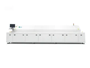
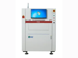
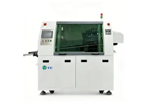
In modern electronic contract manufacturing (EMS) and OEM operations, quality engineering has evolved from reactive post-reflow inspection to proactive in-line quality assurance. Statistical studies across high-density PCB assembly lines reveal that over 70% of all SMT soldering defects—including solder bridging, insufficient solder joints, tombstoning, voiding, and component misalignment—originate directly during the solder paste stencil printing process.
As micro-electronic packaging advances toward 01005 (0402 metric) passive chips, 0.3mm fine-pitch Wafer-Level Chip Scale Packaging (WLCSP), and high-pin-count System-in-Package (SiP) modules, manual visual checks and basic 2D optical systems are no longer mathematically capable of controlling printing quality. Implementing a robust 3D Solder Paste Inspector (SPI) from verified China manufacturers has become a baseline requirement for tier-1 automotive, aerospace, telecom, and consumer electronics factories globally.
Legacy 2D inspection systems rely exclusively on grayscale image intensity to detect solder presence. They fail to measure critical volumetric data, substrate warpage, or height topography. Modern 3D Solder Paste Inspection systems manufactured in China utilize sophisticated optical technology combining Programmable Moiré Phase-Shifting Profilometry (PMP) and dual/quad digital laser projectors.
To eliminate optical shadow effects caused by tall adjacent components or thick stencils, high-end Chinese 3D SPI systems deploy dual or quadruple symmetrical digital light projectors. This delivers shadow-free 3D surface mapping across dense PCBs.
By projecting sinusoidal fringe patterns onto the solder deposit and capturing shifted phase images with ultra-high-resolution telecentric camera lenses, the machine calculates height profile values on every single pixel with sub-micron precision.
Substrate flex and thermal warpage distort height references. Advanced Chinese 3D SPI units feature real-time Z-axis plane tracking that dynamically adjusts height baselines across the board surface, ensuring zero false alarms.
| Parameter / Feature | Legacy 2D SPI Systems | Industrial 3D SPI (China Tier-1 Standard) | IPC Quality Standard Impact |
|---|---|---|---|
| Height Measurement | Not Capable (Estimated via brightness) | Real 3D Profile (Range: 0 - 600 µm, Precision < 0.5 µm) | IPC-7527 Compliance |
| Solder Volume Calculation | Area-based approximation only | Integral 3D Volume Calculation (Accuracy > 99%) | Prevents solder joint starvation/voiding |
| Shadow Effect Mitigation | High risk of illumination blind spots | Dual/Quad Light Projection Angle Compensation | Essential for 0201 / BGA fine pitch |
| Defect Detection Capabilities | Bridging, Missing Paste, Offset (2D) | Volume, Height, Area, Offset, Bridge, Shape, Peak, Coplanarity | Zero defect escape target (Class 3 Electronics) |
| Closed-Loop Printing SPC | Manual inspection log export | Real-time automatic IPC-HERMES feedback to stencil printer | Industry 4.0 Smart Factory Automation |
China has established itself as the global hub for SMT equipment manufacturing, leveraging mature industrial ecosystems in Shenzhen and Guangdong Province. For overseas buyers, importing 3D Solder Paste Inspection systems directly from Chinese OEMs offers distinct technical and financial benefits:
Chinese SPI manufacturers deliver high-end optical components (e.g., German/Japanese industrial cameras and telecentric lenses) paired with locally optimized motion control platforms, reducing capital investment by 40% to 60% compared to Western brands while maintaining equal GR&R metrics.
China's rapid electronics engineering cycle allows domestic manufacturers to swiftly implement software updates, custom AI algorithm models, and specific SMEMA/IPC conveyor protocol extensions tailored to custom factory MES environments.
Rather than buying standalone machines, Chinese supplier networks provide end-to-end line integration—from vision-guided stencil printers to pick-and-place units, multi-zone reflow ovens, dual-rail conveyors, and downstream 3D AOI inspection.
Shenzhen Yichun Electronic Automation Equipment Co., Ltd., founded in 2013, is a practical SMT production line solution provider and integrator focused on helping electronics manufacturers build stable and efficient manufacturing lines.
We specialize in SMT line planning, equipment integration, installation, and technical support based on real factory production requirements. Our solutions combine reliable SMT equipment with practical engineering experience to deliver cost-effective and easy-to-operate production lines for growing manufacturers.
Our main solutions include reflow ovens, wave soldering systems, SMT production lines, automatic printers, pick-and-place machines, and related peripheral equipment. Rather than focusing only on individual machines, we emphasize complete line configuration, factory layout optimization, and long-term operational stability.
Yichun Electronic operates a demonstration and training showroom used for equipment testing, solution verification, and customer visits, helping clients better understand production processes before implementation.

Our solutions are applied in consumer electronics, industrial control, communication products, and automotive electronics. We have supported SMT line projects in regions including Southeast Asia, South Asia, and Eastern Europe, providing installation, technical assistance, and ongoing service support.
To provide practical, stable, and cost-effective SMT automation solutions that help electronics manufacturers improve productivity, maintain consistent product quality, and grow their manufacturing capabilities with confidence.
To become a reliable long-term SMT line integration partner for manufacturers seeking practical solutions, flexible equipment configurations, and dependable engineering support.
We focus on real production needs rather than theoretical configurations. From initial line planning to installation and long-term maintenance, our engineering team provides continuous support throughout the entire manufacturing lifecycle to ensure stable and efficient production.
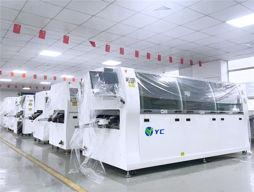
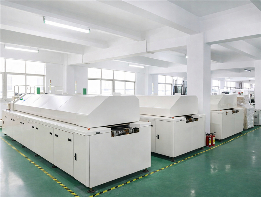
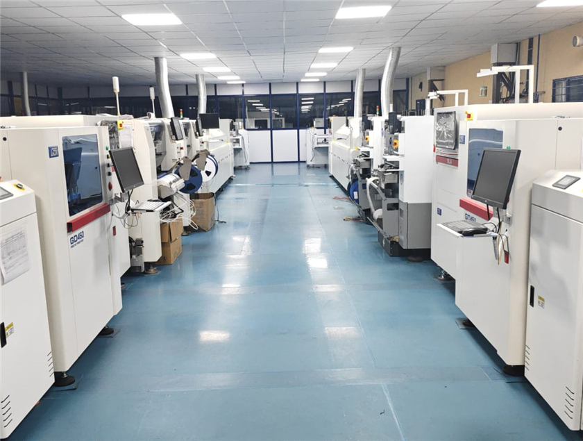
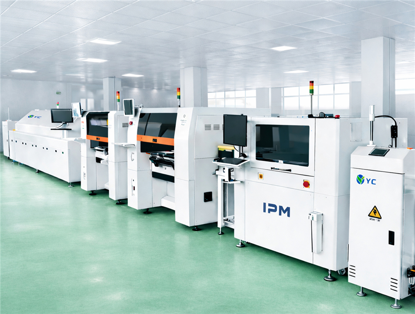
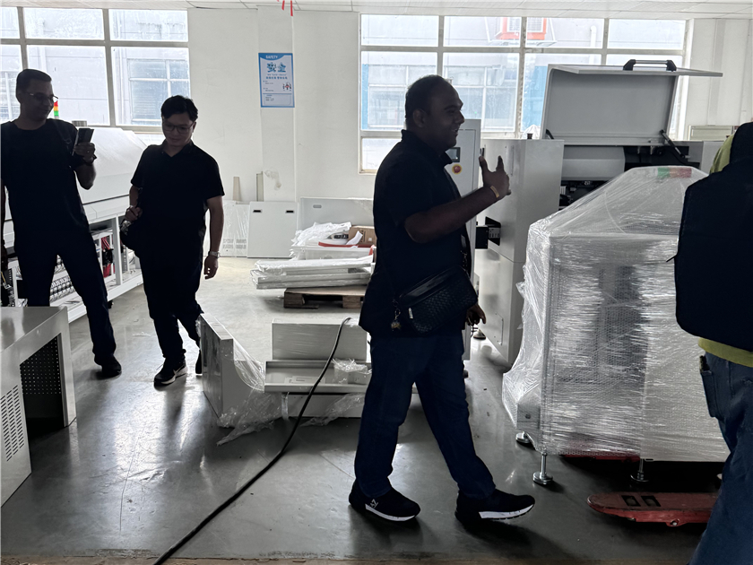
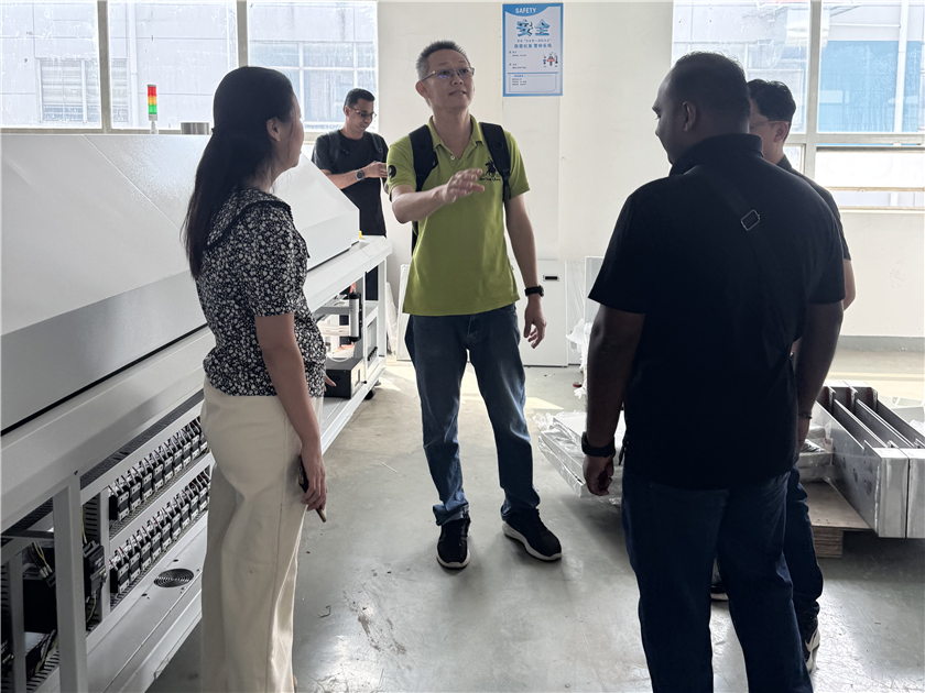
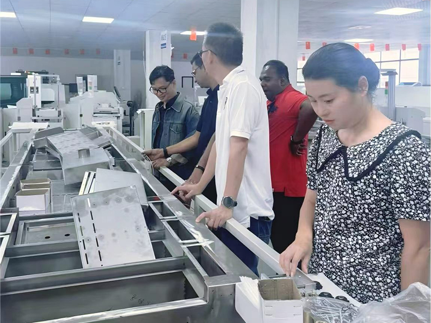
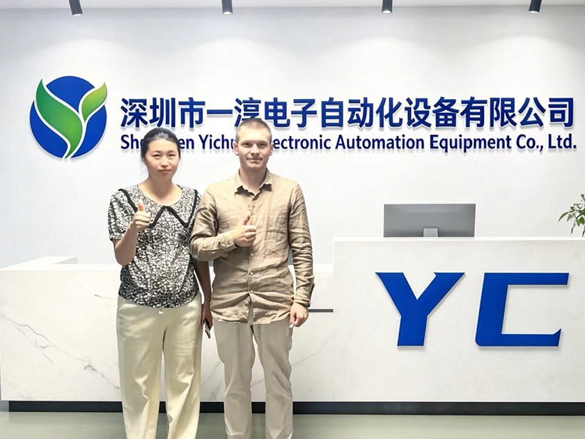
As electronics manufacturing continues to evolve, Yichun Electronic remains focused on delivering practical SMT line solutions that help manufacturers build reliable and efficient production capabilities. We believe stable equipment, realistic engineering design, and long-term technical support are the foundation of successful manufacturing operations.
Whether customers are setting up a new SMT line or optimizing an existing production process, our team is committed to providing straightforward, dependable solutions tailored to real factory needs. We look forward to building long-term partnerships with manufacturers seeking practical, cost-effective SMT production solutions.
3D Solder Paste Inspection is deployed across diverse industrial sectors, each imposing rigorous IPC standards and mathematical acceptance criteria for solder volume deposit accuracy.
Automotive Control Units (ECUs), ADAS radar sensors, and EV Battery Management Systems (BMS) demand zero defect escape. 3D SPI systems verify sub-millimeter paste height profiles on high-reliability thermal pads to prevent field failures under extreme vehicle vibration.
High-frequency base station mainboards incorporate dense arrays of micro-BGA packages and 0201 passives. Precision 3D SPI prevents micro-bridging between adjacent pads and ensures uniform volume distribution across multi-layer RF PCBs.
Surgical monitors, implantable device controllers, and high-voltage power converters require strict adherence to IPC-A-610 Class 3 specifications. In-line 3D SPI provides traceable Statistical Process Control (SPC) audit records for medical regulatory compliance.
Selecting the right 3D Solder Paste Inspector vendor requires systematic engineering evaluation beyond price negotiations. Purchasing directors and quality managers should verify five key technical benchmarks:
Request official GR&R test reports using standard calibration target blocks. A world-class 3D SPI unit must demonstrate GR&R < 10% under tolerance limits, ensuring true measurement consistency regardless of operator or thermal variance.
Verify that the SPI system natively supports IPC-HERMES-9852 and major printer communication protocols (e.g., GKG, DEK, MPM). The system should automatically transmit positional alignment X/Y/theta offsets and trigger stencil cleaning commands upon detecting trend drift.
Inspect camera specifications: Telecentric lenses ensure zero perspective distortion across the entire field of view (FOV). Combine with high-speed CMOS sensors (minimum 5 Megapixels at 60+ FPS) for uncompromised tactile accuracy at full line speeds.
The software suite must generate real-time X-bar R charts, CP/CPK statistical indices, height histogram distribution curves, and export Gerber layer overlay files without requiring expensive recurring monthly software license fees.
Key technical answers compiled by senior SMT manufacturing directors for overseas buyers and plant managers.
2D optical inspection only measures two-dimensional surface area (length and width) and shadow contrast. It cannot calculate solder volume, height profile, or three-dimensional pad coplanar geometry. As component pad pitches shrink to 0.3mm fine-pitch BGA or 01005 passives, a solder deposit can cover the correct area but have insufficient height or excessive thickness. 3D SPI utilizes fringe projection phase shifting to capture precise 3D volumetric metrics, eliminating undetected solder starvation and bridging defects before reflow heating.
3D SPI machines communicate across standardized Ethernet industrial protocols like IPC-HERMES-9852 or SMEMA. When the 3D SPI detects systematic statistical drift in solder registration (e.g., paste deposits creeping +15 µm in the X direction across consecutive boards) or recurring volume dropouts due to clogged stencil apertures, it automatically sends positioning feedback to the automatic stencil printer. The printer then performs micro-adjustments to its servo alignment stages or initiates an automated under-stencil wipe sequence without stopping the line.
Industrial-tier 3D SPI equipment supplied by repute Chinese manufacturers (such as Yichun SMT solutions) complies strictly with Six Sigma quality management frameworks. Systems must achieve a Gauge Repeatability and Reproducibility (GR&R) rating under 10% across repeated measurements on standardized 3D calibration blocks. Height resolution typically reaches down to 0.1 µm, with height measurement accuracy within ±1 µm on a standard 100 µm benchmark block.
Leading Chinese exporters offer comprehensive engineering support packages including remote diagnostic setup via secure VPN, comprehensive video training modules, step-by-step programming manuals based on Gerber files, and local field engineer dispatch through regional distributors in Southeast Asia, Europe, and the Americas. Machine software includes full multi-language user interfaces (English, Spanish, Vietnamese, Russian, Japanese) for instant operator adoption.
Yes. Modern 3D SPI software imports standard RS-274X and Gerber X2 formats directly alongside CAD pick-and-place coordinate data. The CAD/Gerber integration wizard automatically assigns inspection windows (FOVs), identifies component pad boundaries, sets volumetric threshold limits based on stencil thickness, and compiles operational inspection programs in less than 10 minutes.
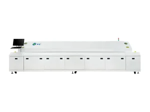
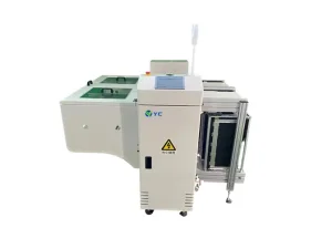
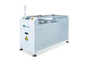
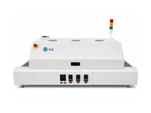
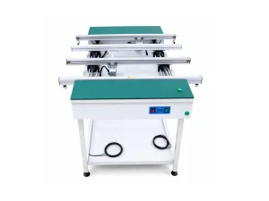
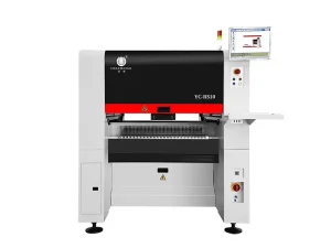
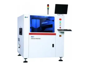
Explore our complete lineup of SMT line auxiliary equipment, automatic PCB loaders/unloaders, reflow ovens, and high-precision mounting systems designed to maximize line efficiency.
The global SMT equipment industry is transitioning toward fully autonomous smart factories. Modern China SPI manufacturers are at the forefront of incorporating Deep Learning AI models into 3D optical inspection workflows:
Machine learning neural networks continuously analyze 3D point cloud height profiles, automatically categorizing solder defects into precise root causes (e.g., stencil aperture clogging vs squeegee pressure imbalance) without operator intervention.
Connecting upstream 3D SPI dataset results with post-reflow 3D AOI inspection records enables predictive AI algorithms to forecast joint reliability, optimizing thermal reflow curves and squeegee speeds in real time.
Multi-factory enterprise managers can monitor real-time CPK yield indices, defect heatmaps, and maintenance schedules across global SMT production lines via centralized cloud management interfaces.
 Yichun Electronic